


Short answer: A resistivity reading of 18 MΩ·cm tells you your deionized water is low in ions. It says nothing about the trace metals that can still ruin a wafer: the sodium, potassium, calcium, iron, and copper a resistivity meter simply cannot see. To actually verify semiconductor-grade DI water, you need a laboratory metals panel run by ICP-MS, measuring those elements down to parts-per-trillion. That’s the test most fabs skip until a finished part comes back contaminated.
If you’ve been treating 18 MΩ·cm as your definition of “clean,” you’re not alone, and you’re not wrong to start there. But resistivity is one number measuring one thing. This guide covers what it misses, which contaminants matter for semiconductor work, the standards that define real purity grades, and how DI water testing fits into water quality testing for semiconductor manufacturing.
Why 18 MΩ·cm isn’t a clean bill of health
Resistivity measures how well water resists an electrical current. Pure water is a poor conductor; dissolved ions make it a better one. A high reading (18.2 MΩ·cm is the theoretical maximum for water at 25°C) means very few charged ions are present.
The catch is that resistivity is a single, bulk measurement. It reflects the total ionic content of the water averaged together, and it cannot isolate or quantify any individual element. A concentration of sodium low enough to leave resistivity pinned near 18.2 MΩ·cm can still be high enough to shift a transistor’s threshold voltage. Resistivity and device-killing metal contamination live on different scales.
That is the gap that catches fabs off guard. Water can read a flawless 18.2 MΩ·cm at the meter and still carry enough sodium to explain a contaminated finished part. Sodium is a particular menace in semiconductor manufacturing because sodium ions are mobile in silicon dioxide and shift the threshold voltage of a device. With enough drift, the transistor stops working as designed.
What semiconductor DI water testing actually measures
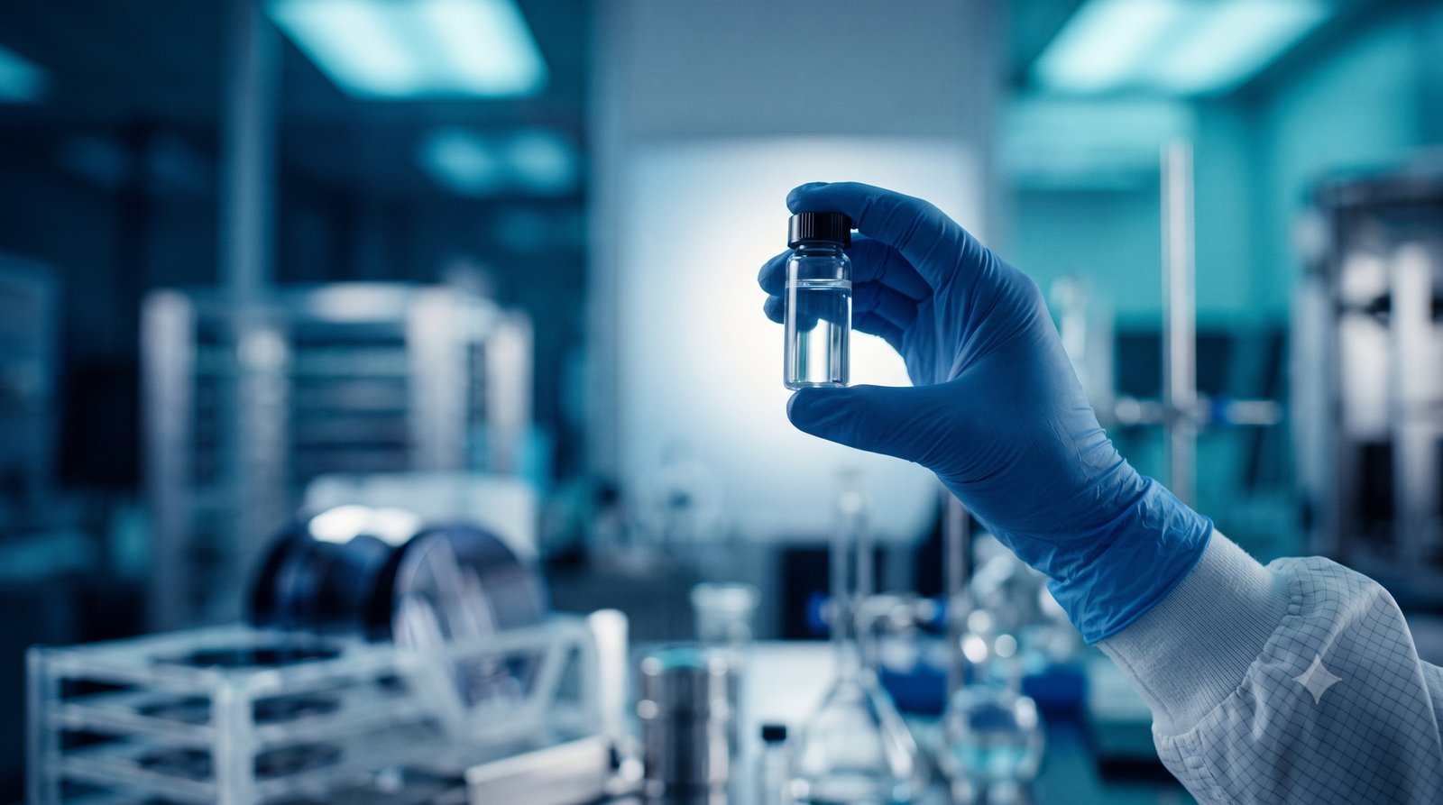
Because resistivity can’t isolate individual elements, verifying semiconductor-grade DI water comes down to a trace-metals panel run by ICP-MS (inductively coupled plasma mass spectrometry), the laboratory method that quantifies a specific metal down to parts-per-trillion. This is the measurement most facilities don’t have in-house, because it needs a lab instrument rather than a handheld probe.
A well-designed panel covers 11 to 16 elements, and the results separate two very different contamination stories.
| Metal group | Elements | What an elevated reading usually points to |
|---|---|---|
| Human-contact metals | Sodium (Na), Potassium (K), Calcium (Ca) | Handling contamination: skin, breath, or a process step where something contacts the water or the part |
| Hardware metals | Iron (Fe), Copper (Cu), Nickel (Ni), Chromium (Cr), Zinc (Zn), Aluminum (Al) | Plumbing, fittings, valves, or equipment in contact with the water |
The human-contact metals usually tell the most revealing story. Skin, breath, and handling all shed sodium and potassium, so an elevated Na, K, or Ca reading frequently points to a sampling, handling, or process step where a part or the water touches something it shouldn’t, rather than a failure of the DI system itself. The hardware metals point instead to the plumbing, fittings, or equipment the water runs through. Separating the two is what lets you find the source instead of guessing.
Concerned about contaminants in your water?
Get water testing from KETOS KELP using EPA-certified methodology, results you can trust, backed by real data.
Order a Water Test →The standards that define semiconductor water grades
Two bodies set the reference points most fabs work against:
ASTM D5127, Standard Guide for Ultra-Pure Water Used in the Electronics and Semiconductor Industries, defines multiple grades of electronics-grade water tied to device line width, so the finer the geometry, the tighter the water spec. It sets recommended limits across a range of parameters, including the individual trace metals that matter most for device yield, at the point of distribution.
SEMI standards cover the manufacturing side: SEMI F63 addresses ultrapure water quality for semiconductor processing, and SEMI E180 specifies how to measure surface metal contamination by ICP-MS. The element list in SEMI E180 (sodium, aluminum, potassium, calcium, iron, copper, nickel, chromium, zinc, and others) is a good template for what a DI water metals panel should include.
You don’t need to memorize the tables. The practical takeaway is that “semiconductor grade” is defined by a spread of parameters across recognized standards, and no single online reading covers all of them. A periodic laboratory panel is how you confirm the water in your loop still matches the grade your process assumes.
How to test your DI water: a practical sequence
If you’ve never validated your DI water from scratch, here’s a sensible order of operations.
- Establish a baseline. Test the water as it comes off your DI system and at the actual point of use. The difference between the two often reveals contamination picked up in the distribution loop.
- Run a full metals panel by ICP-MS. This is the measurement resistivity can’t give you. Prioritize Na, K, and Ca (handling contamination) alongside the hardware metals (Fe, Cu, Ni, Cr, Zn).
- Sample over time, not once. DI water quality drifts as resins load up and filters age. A single clean result is a snapshot; a series across weeks or months tells you whether your system holds spec under real operating conditions.
- Control your sampling. Because Na, K, and Ca are so easy to introduce by hand, how you collect the sample matters as much as the analysis. Use lab-supplied bottles and follow the collection instructions exactly. A contaminated sample produces an alarming number that has nothing to do with your water.
In trace-metals work, sloppy sampling is the most common reason a result looks alarming, which is why the lab you use should supply clean bottles and clear collection instructions.
Testing DI water with KETOS KELP
KETOS KELP is KETOS’s laboratory testing service, built for exactly this kind of verification and for water quality testing in semiconductor manufacturing more broadly. For semiconductor DI water, that means a metals panel run by ICP-MS at the parts-per-trillion sensitivity the application demands, covering the human-contamination elements (Na, K, Ca) and the hardware metals in a single report.
The workflow is straightforward. KETOS KELP provides the sample bottles and collection instructions, so your samples arrive uncontaminated and comparable. You submit samples on a schedule that fits your process (a series over several months is far more informative than a one-off) and get back lab-grade results you can hold against ASTM D5127 and SEMI reference limits. For facilities near the KETOS lab in Sunnyvale, sample drop-off can be arranged in person. KETOS KELP also runs PFAS analysis, if your facility needs to characterize that alongside metals.
KETOS KELP complements your online resistivity monitoring rather than replacing it, adding the one measurement resistivity was never designed to provide: a defensible, standards-referenced picture of the trace metals in your ultrapure water, before they show up in a finished part.
Frequently asked questions
Does 18 MΩ·cm mean my DI water is pure enough for semiconductor use?
Not by itself. Resistivity confirms low ionic content but cannot isolate or quantify individual trace metals. Water can read 18.2 MΩ·cm and still carry enough sodium to affect device performance, which is why a laboratory metals panel is what verifies semiconductor-grade purity.
How do you test for sodium in DI water?
Sodium at semiconductor-relevant levels is measured by ICP-MS (inductively coupled plasma mass spectrometry), which detects individual metals down to parts-per-trillion. A conductivity or resistivity meter cannot isolate sodium or tell you its concentration.
Why are sodium, potassium, and calcium the metals to watch?
They’re the signatures of human contact: skin, breath, and handling all shed them. Elevated Na, K, or Ca in a DI water or finished-part sample frequently points to a handling or sampling step rather than the DI system itself.
What standards apply to semiconductor DI water?
ASTM D5127 defines electronics-grade water quality by device line width. SEMI F63 covers ultrapure water for semiconductor processing, and SEMI E180 specifies ICP-MS measurement of surface metal contamination.
How often should DI water be tested?
Because purity drifts as resins and filters age, periodic sampling beats a single test. A series over weeks or months shows whether your system holds spec under real operating conditions.
Testing your DI water for the first time, or chasing down a contamination you can’t explain? KETOS KELP runs the semiconductor metals panel that resistivity can’t. Talk to the KETOS KELP team.